Table of Contents
① Fact Check
② Is Further Expansion Necessary?
③ Shadows Behind the Power Grid
Lee Jae-myung’s ‘800 Trillion Won Honam Semiconductor’… Samsung Disclosure Cited it as a ‘Candidate Site’
Is the ‘800 Trillion Won Honam Semiconductor’ project unveiled by the Lee Jae-myung administration actually a fact? Judging solely by the government’s announcement, it appears that the decision has already been finalized. The explanation highlighted an investment of 800 trillion won in the southwestern region, the construction of four semiconductor fabs, and the creation of a second semiconductor production hub following the one in the Seoul metropolitan area. The figures were massive, and the message was clear. It sounded like a declaration that the Honam region would no longer be a periphery of industrialization but would become a new pillar on South Korea's semiconductor map.
However, when one examines the corporate regulatory filings, the story changes. Samsung Electronics described the investment in Gwangju not as a confirmed location, but as a ‘candidate site.’ Furthermore, in a revised disclosure, the company added a disclaimer that this mid-to-long-term investment plan is a future projection based on current market conditions and serves as a guideline to aid understanding.
SK Hynix also included a statement indicating that specific schedules and investment plans would be disclosed at a later date, once they are finalized following approval by the board of directors. A distinct discrepancy in tone has emerged between the government’s definitive announcement and the companies' conditional disclosures.
Verdict: Omission of Conditions and Exaggeration
Both the government announcement and the corporate disclosures provide the basis for the ‘800 Trillion Won Honam Semiconductor’ concept. However, neither Samsung nor SK Hynix filings frame these as confirmed investments. Conditions such as ‘candidate site,’ ‘future plan,’ ‘guideline,’ ‘subject to change,’ and ‘board approval’ were attached.
Therefore, while the Lee Jae-myung administration’s explanation contains elements of truth, it is heavily characterized by the omission of conditions and exaggeration, leading the public to perceive it as a confirmed investment.
On June 29, the Ministry of Trade, Industry and Energy announced at the ‘National Report on the 3 Major Megaprojects for South Korea’s Great Leap Forward,’ held at the Blue House Guest House, that it had discussed large-scale investment plans in three major fields—semiconductors, physical AI, and AI data centers—as well as plans to expand power and location infrastructure.
The very title of the government’s announcement was “Construction of 800 Trillion Won Semiconductor Fabs in the Southwest Region, Cultivation of Packaging Hubs with 81 Trillion Won Investment in the Chungcheong Region.” The main text also explained that it would build four 800-trillion-won-scale semiconductor fabs in the southwest, along with an ecosystem of partners and human resources, to establish a second production hub following the capital region.
The government’s language was strong. Terms like ‘unprecedented investment,’ ‘second production hub,’ and ‘four semiconductor fabs’ are easily interpreted by readers and the public as if the large-scale investment decisions by major private companies had essentially been finalized. In fact, numerous media outlets reported that Samsung Electronics and SK Hynix were planning to build four or more advanced semiconductor front-end process fabs in the Gwangju and Jeonnam regions, with a total value of 800 trillion won.
The government described this as a core pillar of its semiconductor speed, hub, and leadership strategies, while Lee Jae-myung highlighted it as a symbol of the nation’s great leap forward.
However, there was a decisive caveat in Samsung’s official explanation. Samsung Electronics’ semiconductor newsroom, while explaining the company’s domestic investment plans, stated that it planned to invest a total of 425 trillion won in the Honam region, with 400 trillion won specifically for semiconductors. At the same time, it mentioned pursuing the construction of a new semiconductor fab and building a digital twin-based innovation hub in Gwangju.
But it immediately added, “We are planning for Gwangju as a candidate site, as we expect many incentive supports such as power, water supply, securing and training human resources, and living conditions among several regions.” Gwangju was a ‘candidate site,’ not a confirmed location.
The remarks of Samsung Electronics Chairman Lee Jae-yong were in the same vein. According to an MBC report, Chairman Lee stated, “We are planning for Gwangju as a candidate site, as we expect many incentive supports such as power, water, securing personnel, and various infrastructure among several regions.” While an interpretation that it was ‘chosen’ is possible, the Chairman’s own expression was ‘candidate site.’ This differs from the definitive language used in the government’s announcement.
More importantly, there are the regulatory filings.
While corporate press releases may be promotional documents, regulatory filings are legal documents intended for the market and shareholders. Samsung Electronics’ revised disclosure on future business and management plans included the phrase, “The scale and schedule are subject to change in the future,” and added, “The aforementioned mid-to-long-term investment plan is a future plan based on current market conditions and is provided as a guideline to aid understanding; it may fluctuate depending on future market conditions and changes in the company’s management environment.”
This sentence is a defensive statement that explains the scope and conditions of potential investment rather than a confirmation of investment.
SK Hynix’s disclosure was to a similar effect. According to the same report, while SK Hynix listed the Yongin semiconductor cluster, the Cheongju production base, and the southwestern cluster, it stated that these investment plans were guidelines intended to aid understanding and were subject to change based on market conditions and management environment shifts.
In particular, it explained that specific schedules and investment plans would be disclosed later at the time they are finalized through board approval. This means that final board approval and concrete schedules remain to be determined.
This is the core of this fact-check.
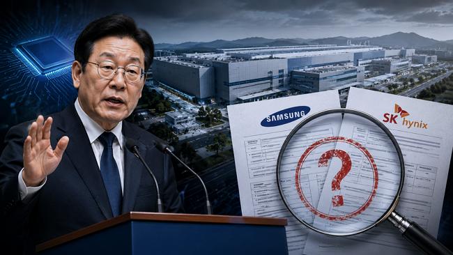 A question mark placed over the Samsung and SK Hynix disclosure documents questions the facts behind the ‘800 Trillion Won Honam Semiconductor’ announcement. The government announced it in definitive language, but corporate disclosures left room for future plans, candidate status, and potential changes. [Photo = Hanmi Ilbo Graphic]
The Issue is Distortion of Facts, Not Just Promotion
Disclosures on future business and management plans do not always contain only confirmed investments. It is common for large corporations to inform the market of their mid-to-long-term strategies and to include disclaimers that the scale and timing of investments may change. However, this case is different because it was announced as a national ‘great leap forward’ project at a presidential national report session.
If the government packaged a private company’s conditional mid-to-long-term guideline as a confirmed national project, this goes beyond simple promotion and becomes a matter of distorting facts.
In particular, the fact that Gwangju is a ‘candidate site’ is significant. The location of a semiconductor fab is only confirmed when power, water, ultra-pure water, wastewater treatment, human resources, partner companies, logistics, customer certification, and local government incentives are all aligned. A candidate site is, literally, just a candidate. If the government announced a candidate site as a confirmed location and explained a future plan as a fixed investment decision, the public was not told the key conditions.
Therefore, the answer to the question, “Is Lee Jae-myung’s 800 trillion won Honam semiconductor project true?” is not a simple yes or no. The numbers were there. The announcement happened. The companies did put forward mid-to-long-term investment concepts. However, rather than confirmed investments, these were future plans that could change depending on market conditions, management environments, infrastructure requirements, and board approval.
If the government’s announcement did not sufficiently explain these conditions, the ‘800 Trillion Won Honam Semiconductor’ project can be viewed as an exaggerated political message cloaked in the guise of fact.
In political circles, this is bound to raise arguments about ‘lies.’ However, in the language of fact-checking, the crux of the matter is the ‘omission of conditions and exaggeration.’ The President’s words sounded like a confirmation, while the companies’ disclosures said it was not yet finalized. One of the two was not accurately explained to the public.
If the Honam semiconductor project is a truly necessary and viable investment, there is no reason for the government to hide it. It could simply disclose whether Samsung and SK have received board approval, the specific investment timing, product mix, long-term supply contracts, plans for securing power and water, and the distinction between corporate burdens and government support. However, what has been confirmed so far is just a massive 800 trillion won figure and the numerous conditions attached to it.
Is the Lee Jae-myung administration’s ‘800 Trillion Won Honam Semiconductor’ a confirmed investment decision, or a political blueprint of the administration?
The conclusion of this primary fact-check is clear: the government’s announcement contains some facts, but it omitted key conditions. Therefore, this expression is closer to ‘omission of conditions and exaggeration’ than it is to ‘fact.’
The next question is more fundamental: Even if the Honam semiconductor project could be pursued conditionally, does South Korea truly need an additional four memory fabs right now? Does the projected memory shortage in 2026 provide sufficient grounds for four new fabs in the 2030s? In Part 2, Hanmi Ilbo will examine this industrial necessity.

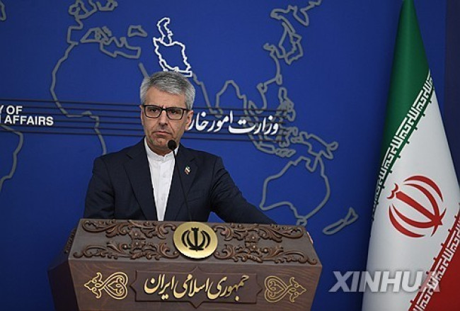 Iranian Foreign Ministry: "Continuing Message Exchanges with the U.S. and Activities of Mediating Countries"
Esmaeil Baghaei, Spokesperson for the Iranian Ministry of Foreign Affairs [Xinhua, Yonhap News file photo]Esmaeil Baghaei, spokesperson for the Iranian Ministry of Foreign Affairs, stated on the 26th
Iranian Foreign Ministry: "Continuing Message Exchanges with the U.S. and Activities of Mediating Countries"
Esmaeil Baghaei, Spokesperson for the Iranian Ministry of Foreign Affairs [Xinhua, Yonhap News file photo]Esmaeil Baghaei, spokesperson for the Iranian Ministry of Foreign Affairs, stated on the 26th
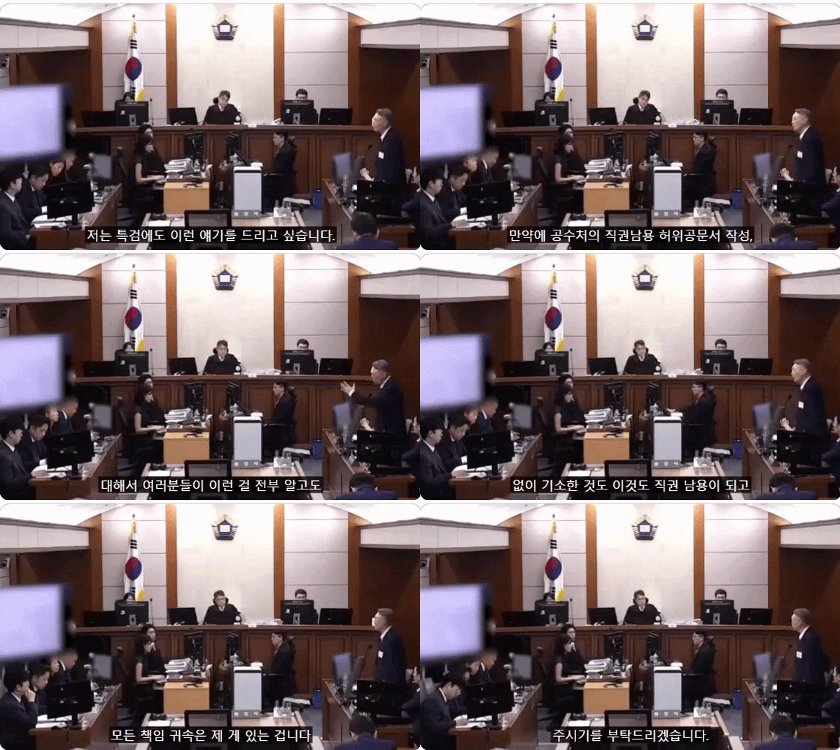 President Yoon: "Do You Think You Are Safe from the Special Counsel?"... Final Statement Video Released
President Yoon Suk Yeol rebuking the special prosecutor on the 24th. [Court video / @birds_justice X account subtitle GIF] A video of President Yoon Suk Yeol's closing statement at his trial rega
President Yoon: "Do You Think You Are Safe from the Special Counsel?"... Final Statement Video Released
President Yoon Suk Yeol rebuking the special prosecutor on the 24th. [Court video / @birds_justice X account subtitle GIF] A video of President Yoon Suk Yeol's closing statement at his trial rega
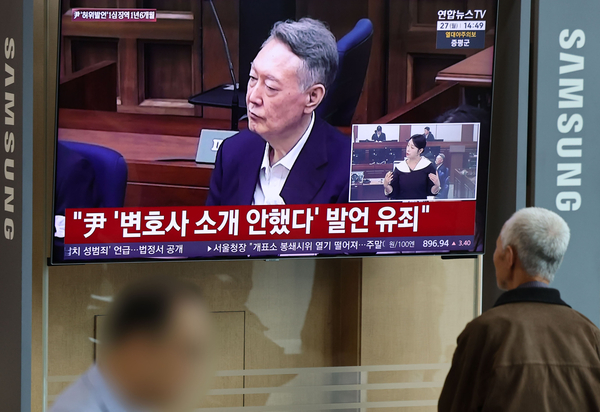 President Yoon, regarding the first-instance ruling on the Public Official Election Act: “An excessive political verdict that distorts the facts… We will appeal immediately.”
The first-instance sentencing hearing for President Yoon Suk Yeol regarding violations of the Public Official Election Act is being broadcast live at Seoul Station on the 27th. [Photo=Yonhap News]Pres
President Yoon, regarding the first-instance ruling on the Public Official Election Act: “An excessive political verdict that distorts the facts… We will appeal immediately.”
The first-instance sentencing hearing for President Yoon Suk Yeol regarding violations of the Public Official Election Act is being broadcast live at Seoul Station on the 27th. [Photo=Yonhap News]Pres
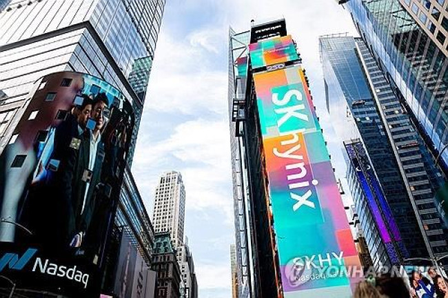 WSJ: "SK Hynix ADR Premium Is a Sign of AI Trading Overheat"
Advertisement for SK Hynix ADR listing in New York's Times Square [Reuters=Yonhap News file photo]The Wall Street Journal (WSJ) has pointed out that the price of SK Hynix’s American Depositary Recei
WSJ: "SK Hynix ADR Premium Is a Sign of AI Trading Overheat"
Advertisement for SK Hynix ADR listing in New York's Times Square [Reuters=Yonhap News file photo]The Wall Street Journal (WSJ) has pointed out that the price of SK Hynix’s American Depositary Recei
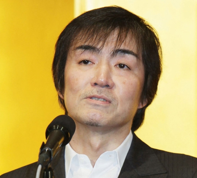 'Godfather of Japanese Mystery Novels' Keigo Higashino Passes Away After Battle with Cancer at 68
Famous Japanese mystery novelist Keigo Higashino [AFP=Yonhap News]It has been belatedly reported that Keigo Higashino, the "godfather of Japanese mystery novels" and author of bestsellers such as "The
'Godfather of Japanese Mystery Novels' Keigo Higashino Passes Away After Battle with Cancer at 68
Famous Japanese mystery novelist Keigo Higashino [AFP=Yonhap News]It has been belatedly reported that Keigo Higashino, the "godfather of Japanese mystery novels" and author of bestsellers such as "The
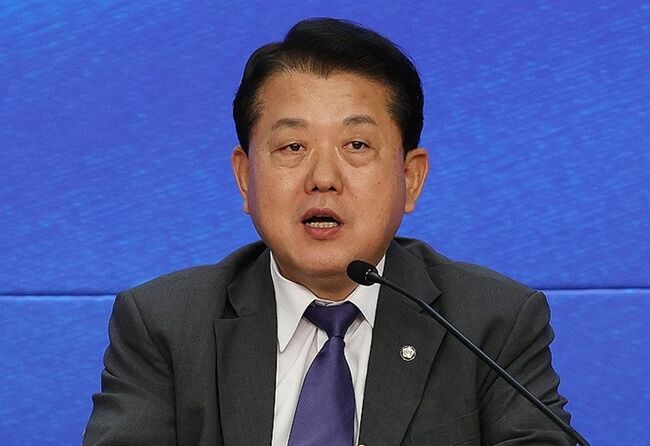 [Park Pil-kyu Security Column] To the Ignorant Trying to Clothe a Beast in Sheep's Clothing
Rep. Kim Byung-joo of the Democratic Party of Korea [Photo=Yonhap News]“The Air Force Academy doesn't teach you how to fly a plane!” “The Army, Navy, and Air Force academies are exactly the
[Park Pil-kyu Security Column] To the Ignorant Trying to Clothe a Beast in Sheep's Clothing
Rep. Kim Byung-joo of the Democratic Party of Korea [Photo=Yonhap News]“The Air Force Academy doesn't teach you how to fly a plane!” “The Army, Navy, and Air Force academies are exactly the
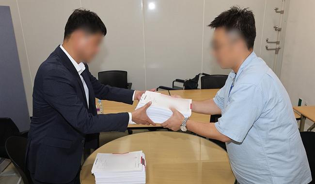 [Issue Diagnosis] Two Effects of the Election Petition Review
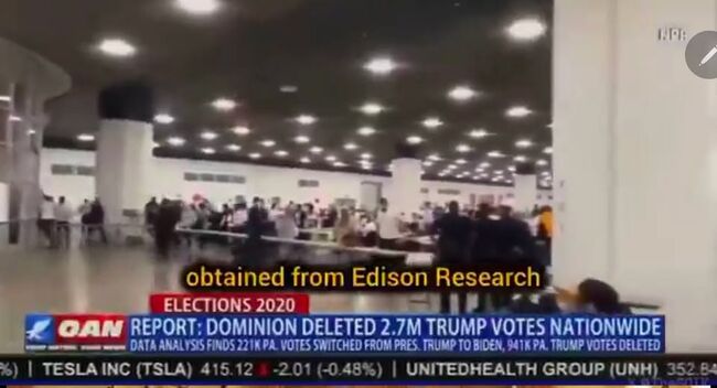 [Photo] Evidence of Election Fraud Flooding U.S. Media… Trump Had 2.7 Million Votes Stolen
 [Video] U.S. Semiquincentennial Air Show... 'Art in the Sky' streaks across New York
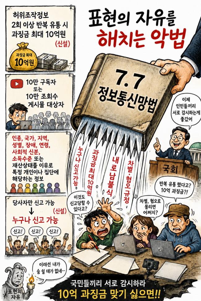 [Editorial Cartoon] A Draconian Law That Undermines Freedom of Expression

 List
List